Difference between revisions of "OpenM128 User Manual"
| (9 intermediate revisions by the same user not shown) | |||
| Line 1: | Line 1: | ||
| − | |||
== Overview == | == Overview == | ||
| − | ::This user manual contains schematic and demo of Waveshare OpenM128 development board. It helps you to quick start your AVR development. | + | ::This user manual contains schematic and demo of Waveshare OpenM128<ref>[http://www.waveshare.com/catalogsearch/result/?q=openm128 OpenM128 development board]</ref> development board. It helps you to quick start your AVR development. |
== Hardware design == | == Hardware design == | ||
| Line 9: | Line 8: | ||
::First of all, we start from the common LED demo. This demo is an example of flashing alternately LED, controlled by the MCU. How do the MCU finish such a common demo? And what circuit work together? | ::First of all, we start from the common LED demo. This demo is an example of flashing alternately LED, controlled by the MCU. How do the MCU finish such a common demo? And what circuit work together? | ||
| − | ::For the MCU system, actually its program controls the I/O pins to output high or low to turn on or turn off the LEDs. And the time span of the high or low output controls the time span of light up. Surely, the chip needs power supply to work; it needs clock circuit to control LED blink time; it needs Download/Configure circuits to | + | ::For the MCU system, actually its program controls the I/O pins to output high or low to turn on or turn off the LEDs. And the time span of the high or low output controls the time span of light up. Surely, the chip needs power supply to work; it needs clock circuit to control LED blink time; it needs Download/Configure circuits to program the compiled project; it needs reset circuits to reset and begin again. The pins of chip can be divided into I/O, SPI, I2C, USART interfaces and so on according to the features. |
::Power supply circuit, a clock circuit, reset circuit and configuration circuit in above-mentioned are the necessary circuits of MCU development. So, many minimum system board just have these circuits and won't extend other feature interfaces. However, OpenM128 extends all chip interfaces of different kinds and gives you supporting function modules and drivers. Helps you to quick start all feature interfaces learning and to develop similar extends. A variety of circuits will be introduced in the following chapter. | ::Power supply circuit, a clock circuit, reset circuit and configuration circuit in above-mentioned are the necessary circuits of MCU development. So, many minimum system board just have these circuits and won't extend other feature interfaces. However, OpenM128 extends all chip interfaces of different kinds and gives you supporting function modules and drivers. Helps you to quick start all feature interfaces learning and to develop similar extends. A variety of circuits will be introduced in the following chapter. | ||
| Line 15: | Line 14: | ||
=== Power Supply Circuit === | === Power Supply Circuit === | ||
| − | ::Power supply circuit is the basic circuit to drive OpenM128 development board. We can find that ATmega128A-AU works on 2.7V~5.5V in the datasheet. And the board is designed for both 5V and 3.3V. The AMS1117-3.3 onboard is used for converting 5V to 3.3V, you can set the jumper to convert the MCU input voltage between 3.3V and 5V. In addition, the power supply circuit contains control switch, power LED, 3.3V/5V/GND pin out, that make control and inspection of power supply circuit more easily.<br/> | + | ::Power supply circuit is the basic circuit to drive OpenM128 development board. We can find that ATmega128A-AU works on 2.7V~5.5V in the datasheet<ref>[http://www.atmel.com/images/atmel-8151-8-bit-avr-atmega128a_datasheet.pdf ATmega128A datasheet]</ref>. And the board is designed for both 5V and 3.3V. The AMS1117-3.3 onboard is used for converting 5V to 3.3V, you can set the jumper to convert the MCU input voltage between 3.3V and 5V. In addition, the power supply circuit contains control switch, power LED, 3.3V/5V/GND pin out, that make control and inspection of power supply circuit more easily.<br/> |
[[File:OpenM128-Power-Supply-Circuit.png|600px]] | [[File:OpenM128-Power-Supply-Circuit.png|600px]] | ||
| Line 70: | Line 69: | ||
=== Download/configure circuit === | === Download/configure circuit === | ||
| − | ::Download, also known as programming, is a chip programming and configuration process. AVR MCUs support ISP, JTAG, PDI download and so on. The first two are more commonly used. OpenM128 extends 2 kinds of download interface, they are a 10-pin-ISP, a 6-pin-ISP and a 10-pin-JTAG. You can connect standard AVR programmer or debugger on it directly. You can download by JTAG or ISP, but only the JTAG interface supports both download and on-chip debug.<br/> | + | ::Download, also known as programming, is a chip programming and configuration process. AVR MCUs support ISP, JTAG, PDI download and so on. The first two are more commonly used. OpenM128 extends 2 kinds of download interface, they are a 10-pin-ISP, a 6-pin-ISP and a 10-pin-JTAG. You can connect standard AVR programmer or debugger<ref>[http://www.waveshare.com/product/mcu-tools/avr/programmers-debuggers.htm AVR programmer or debugger]</ref> on it directly. You can download by JTAG or ISP, but only the JTAG interface supports both download and on-chip debug.<br/> |
[[File:OpenM128-Download-Circuit.png|450px]] | [[File:OpenM128-Download-Circuit.png|450px]] | ||
| Line 81: | Line 80: | ||
| MOSI || ISP, master out slave in (serial peripheral interface) | | MOSI || ISP, master out slave in (serial peripheral interface) | ||
|- | |- | ||
| − | | SCK || ISP, Serial | + | | SCK || ISP, Serial Clock,ISP operation is synchronous to SCK. |
|- | |- | ||
| TDI || JTAG, JTAG Test Data In: Serial input data to be shifted in to the Instruction Register or Data Register(scan chains). | | TDI || JTAG, JTAG Test Data In: Serial input data to be shifted in to the Instruction Register or Data Register(scan chains). | ||
| Line 115: | Line 114: | ||
Steps<br /> | Steps<br /> | ||
#<font color="red">Take away</font> the jumper 12864 JMP | #<font color="red">Take away</font> the jumper 12864 JMP | ||
| − | #Connect 2.2inch 320x240 Touch LCD (A) to LCD interface. | + | #Connect 2.2inch 320x240 Touch LCD (A)<ref name="2.2inch 320x240 Touch LCD (A)">[http://www.waveshare.com/2.2inch-320x240-Touch-LCD-A.htm 2.2inch 320x240 Touch LCD (A)]: Please click in [http://www.waveshare.com/product/modules/oleds-lcds/graphic-lcd.htm Graphic-Lcd] for more details about touch LCD.</ref> to LCD interface. |
#Power up and download the program. | #Power up and download the program. | ||
| Line 137: | Line 136: | ||
Steps<br /> | Steps<br /> | ||
#<font color="red">Take away</font> the jumper 12864 JMP | #<font color="red">Take away</font> the jumper 12864 JMP | ||
| − | #Connect 2.2inch 320x240 Touch LCD (A) to LCD interface | + | #Connect 2.2inch 320x240 Touch LCD (A)<ref name="2.2inch 320x240 Touch LCD (A)">[http://www.waveshare.com/2.2inch-320x240-Touch-LCD-A.htm 2.2inch 320x240 Touch LCD (A)]: Please click in [http://www.waveshare.com/product/modules/oleds-lcds/graphic-lcd.htm Graphic-Lcd] for more details about touch LCD.</ref> to LCD interface. |
#Power up and download the program. | #Power up and download the program. | ||
| Line 158: | Line 157: | ||
Steps<br /> | Steps<br /> | ||
#Check the LED jumper position on the board, jumpers LED JMP on. | #Check the LED jumper position on the board, jumpers LED JMP on. | ||
| − | #Connect 8 Push Buttons module to the GPIO interface. | + | #Connect 8 Push Buttons<ref>[[8 Push Buttons]]</ref> module to the GPIO interface. |
#Power up and download the program. | #Power up and download the program. | ||
| Line 177: | Line 176: | ||
Steps<br /> | Steps<br /> | ||
| − | #Connect 8 SEG LED Board to 16 I/Os port. | + | #Connect 8 SEG LED Board<ref>[[8 SEG LED Board]]</ref> to 16 I/Os port. |
#Power up and download the program. | #Power up and download the program. | ||
| Line 196: | Line 195: | ||
Steps<br /> | Steps<br /> | ||
| − | #Connect AD Keypad to ADC interface. | + | #Connect AD Keypad<ref>[[AD Keypad]]</ref> to ADC interface. |
| − | #Connect PL2303 USB UART Board (mini) to USART0. | + | #Connect PL2303 USB UART Board (mini)<ref>[[PL2303 USB UART Board (mini)]]</ref> to USART0. |
#Power up and download the program. | #Power up and download the program. | ||
#Check your COM port and set baud rate to 9600. | #Check your COM port and set baud rate to 9600. | ||
| Line 219: | Line 218: | ||
Steps<br /> | Steps<br /> | ||
| − | #Connect AT24CXX EEPROM Board to I2C interface. | + | #Connect AT24CXX EEPROM Board<ref>[[AT24CXX EEPROM Board]]</ref> to I2C interface. |
#Connect PL2303 USB UART Board (mini) | #Connect PL2303 USB UART Board (mini) | ||
#Power up and download the program. | #Power up and download the program. | ||
| Line 242: | Line 241: | ||
Steps<br /> | Steps<br /> | ||
| − | #Connect PCF8563 RTC Board to I2C interface | + | #Connect PCF8563 RTC Board<ref>[[PCF8563 RTC Board]]</ref> to I2C interface |
#Connect PL2303 USB UART Board (mini) | #Connect PL2303 USB UART Board (mini) | ||
#Power up and download the program. | #Power up and download the program. | ||
| Line 264: | Line 263: | ||
Steps<br /> | Steps<br /> | ||
| − | #<font color="red">Take away</font> the output-power-supply jumper from FT245 USB FIFO Board. | + | #<font color="red">Take away</font> the output-power-supply jumper from FT245 USB FIFO Board <ref>[[FT245 USB FIFO Board (mini)]]</ref>. |
#Connect PC0~PC7 to LED0~LED7 with jumper wire. | #Connect PC0~PC7 to LED0~LED7 with jumper wire. | ||
#Connect the pin side of FT245 USB FIFO Board to 16 I/Os interface and the USB side to PC. | #Connect the pin side of FT245 USB FIFO Board to 16 I/Os interface and the USB side to PC. | ||
| Line 343: | Line 342: | ||
Steps<br /> | Steps<br /> | ||
#Jumper 12864 JMP ON. <font color="red">Warning: jumper VCC should be set to 3.3V, or too large voltage will cause LCD too bright and burned.</font> | #Jumper 12864 JMP ON. <font color="red">Warning: jumper VCC should be set to 3.3V, or too large voltage will cause LCD too bright and burned.</font> | ||
| − | #Connect LCD12864 to LCD interface. | + | #Connect LCD12864<ref>[http://www.waveshare.com/lcd12864-st-3.3v-blue.htm LCD12864-ST (3.3V Blue Backlight)]</ref> to LCD interface. |
#Power up and download the program. | #Power up and download the program. | ||
| Line 381: | Line 380: | ||
Steps<br /> | Steps<br /> | ||
| − | #Connect DS18B20+ to ONE WIRE port<font color="red">Warning: Please make sure DS18B20+ is connected correctly to the ONE WIRE port, Arc side of DS18B20+ must match the sign of ONE WIRE port. Do NOT connect it reversely, or it may be burned. | + | #Connect DS18B20+ to ONE WIRE port. <font color="red">Warning: Please make sure DS18B20+ is connected correctly to the ONE WIRE port, Arc side of DS18B20+ must match the sign of ONE WIRE port. Do NOT connect it reversely, or it may be burned. |
</font> | </font> | ||
#Connect PL2303 USB UART Board (mini). | #Connect PL2303 USB UART Board (mini). | ||
| Line 429: | Line 428: | ||
Steps<br /> | Steps<br /> | ||
| − | #Connect AT45DBXX DataFlash Board to SPI interface | + | #Connect AT45DBXX DataFlash Board<ref>[[AT45DBXX DataFlash Board]]</ref> to SPI interface |
#Connect PL2303 USB UART Board (mini). | #Connect PL2303 USB UART Board (mini). | ||
#Power up and download the program. | #Power up and download the program. | ||
| Line 454: | Line 453: | ||
Steps<br /> | Steps<br /> | ||
#Prepare two OpenM128 and two NRF24L01 boards, for sending, TX, and receiving, RX, data. The following is an example of 2 OpenM128 boards. | #Prepare two OpenM128 and two NRF24L01 boards, for sending, TX, and receiving, RX, data. The following is an example of 2 OpenM128 boards. | ||
| − | #Connect two NRF24L01 RF Boards to the SPI interface of OpenM128 boards separately. | + | #Connect two NRF24L01 RF Boards<ref>[[NRF24L01 RF Board (B)]]</ref> to the SPI interface of OpenM128 boards separately. |
#Connect the RX board to a PC via PL2303 USB UART Board. | #Connect the RX board to a PC via PL2303 USB UART Board. | ||
#Power up and download the program. | #Power up and download the program. | ||
Latest revision as of 02:09, 23 May 2015
Overview
- This user manual contains schematic and demo of Waveshare OpenM128[1] development board. It helps you to quick start your AVR development.
Hardware design
- This chapter mainly about a basic idea of the hardware design of OpenM128. Go with you to witness how a ATmega128A-AU chip becomes OpenM128 board.
- First of all, we start from the common LED demo. This demo is an example of flashing alternately LED, controlled by the MCU. How do the MCU finish such a common demo? And what circuit work together?
- For the MCU system, actually its program controls the I/O pins to output high or low to turn on or turn off the LEDs. And the time span of the high or low output controls the time span of light up. Surely, the chip needs power supply to work; it needs clock circuit to control LED blink time; it needs Download/Configure circuits to program the compiled project; it needs reset circuits to reset and begin again. The pins of chip can be divided into I/O, SPI, I2C, USART interfaces and so on according to the features.
- Power supply circuit, a clock circuit, reset circuit and configuration circuit in above-mentioned are the necessary circuits of MCU development. So, many minimum system board just have these circuits and won't extend other feature interfaces. However, OpenM128 extends all chip interfaces of different kinds and gives you supporting function modules and drivers. Helps you to quick start all feature interfaces learning and to develop similar extends. A variety of circuits will be introduced in the following chapter.
Power Supply Circuit
- Power supply circuit is the basic circuit to drive OpenM128 development board. We can find that ATmega128A-AU works on 2.7V~5.5V in the datasheet[2]. And the board is designed for both 5V and 3.3V. The AMS1117-3.3 onboard is used for converting 5V to 3.3V, you can set the jumper to convert the MCU input voltage between 3.3V and 5V. In addition, the power supply circuit contains control switch, power LED, 3.3V/5V/GND pin out, that make control and inspection of power supply circuit more easily.
- Power supply circuit is the basic circuit to drive OpenM128 development board. We can find that ATmega128A-AU works on 2.7V~5.5V in the datasheet[2]. And the board is designed for both 5V and 3.3V. The AMS1117-3.3 onboard is used for converting 5V to 3.3V, you can set the jumper to convert the MCU input voltage between 3.3V and 5V. In addition, the power supply circuit contains control switch, power LED, 3.3V/5V/GND pin out, that make control and inspection of power supply circuit more easily.
| Pin Name | Description |
|---|---|
| 5V | 5V supply input, it can be used as MCU or other peripherals VCC power supply. |
| 3.3V | 3.3V supply from AMS1117-3.3, it can be used as MCU or other peripherals VCC power supply. |
| GND | Ground |
| VCC | It is a pin corresponding to MCU VCC, you can set the jumper to convert the MCU input voltage between 3.3V and 5V. |
| PWR_5V | 5V input from a power supply. |
Clock Circuit
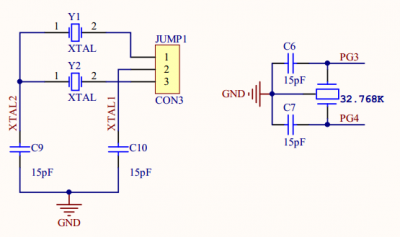
- There is a calibrated RC oscillator in the AVR MCU. So usually, extended clock circuit can be removed under less demanding circumstances on clock accuracy. For higher clock accuracy demand, OpenM128 is designed relative flexibly, it supplies optional oscillator crystal ports besides of onboard 7.3728M and 32.768K crystal. If the MCU RC oscillator is not suit your requirement, you can connect a right crystal and set the XTALn jumper to switch between XTAL1 and XTAL2.(Note: the corresponding fuse bit should be set by the program.)
- There is a calibrated RC oscillator in the AVR MCU. So usually, extended clock circuit can be removed under less demanding circumstances on clock accuracy. For higher clock accuracy demand, OpenM128 is designed relative flexibly, it supplies optional oscillator crystal ports besides of onboard 7.3728M and 32.768K crystal. If the MCU RC oscillator is not suit your requirement, you can connect a right crystal and set the XTALn jumper to switch between XTAL1 and XTAL2.(Note: the corresponding fuse bit should be set by the program.)
| Pin Name | Description |
|---|---|
| XTAL1 | Inverting oscillator amplifier and on-chip clock operating circuit input |
| XTAL2 | Inverting oscillator amplifier output |
| PG3 | I/O pin, it can also be used as 32kHz crystal input |
| PG4 | I/O pin, it can also be used as 32kHz crystal input |
Reset Circuit
- Reset of AVR chip is low active, mean while that a 50 ns low signal input to reset pin will cause the chip reset. When you press the reset button, reset pin connects to negative power supply, and then, when you release the button, although the reset pin convert to high, actually the pressing time is more than 100 ms usually, it was enough for chip reset pulse transmission.
- Reset of AVR chip is low active, mean while that a 50 ns low signal input to reset pin will cause the chip reset. When you press the reset button, reset pin connects to negative power supply, and then, when you release the button, although the reset pin convert to high, actually the pressing time is more than 100 ms usually, it was enough for chip reset pulse transmission.
| Pin Name | Description |
|---|---|
| nRST | Chip reset, low active |
Download/configure circuit
- Download, also known as programming, is a chip programming and configuration process. AVR MCUs support ISP, JTAG, PDI download and so on. The first two are more commonly used. OpenM128 extends 2 kinds of download interface, they are a 10-pin-ISP, a 6-pin-ISP and a 10-pin-JTAG. You can connect standard AVR programmer or debugger[3] on it directly. You can download by JTAG or ISP, but only the JTAG interface supports both download and on-chip debug.
- Download, also known as programming, is a chip programming and configuration process. AVR MCUs support ISP, JTAG, PDI download and so on. The first two are more commonly used. OpenM128 extends 2 kinds of download interface, they are a 10-pin-ISP, a 6-pin-ISP and a 10-pin-JTAG. You can connect standard AVR programmer or debugger[3] on it directly. You can download by JTAG or ISP, but only the JTAG interface supports both download and on-chip debug.
| Pin Name | Description |
|---|---|
| MISO | ISP, master in slave out (serial peripheral interface) |
| MOSI | ISP, master out slave in (serial peripheral interface) |
| SCK | ISP, Serial Clock,ISP operation is synchronous to SCK. |
| TDI | JTAG, JTAG Test Data In: Serial input data to be shifted in to the Instruction Register or Data Register(scan chains). |
| TDO | JTAG, JTAG Test Data Out: Serial output data from Instruction Register or Data Register. |
| TMS | JTAG, JTAG Test Mode Select: This pin is used for navigating through the TAP-controller state machine. |
| TCK | JTAG, JTAG Test Clock: JTAG operation is synchronous to TCK. |
Extension Circuit
- OpenM128 has various expansion circuit and the onboard LED, button ... make I/O operation easily; Some extensions, such as LCD, 16I/O, USART, PWM, I2C, SPI and so on, are not only the literal meaning for beginners. If you master these function interfaces, you will realize infinite charm from SCM. Many available powerful peripheral modules, GPS, WIFI, Graphic, Vedio, Intelligent recognition, can be interfaced to a variety of MCU. If all these modules were integrated into your development board, what surprising thing will you make!
Basic Operation
Power Up and Download
- Connect the programmer to your OpenM128 as shown in the following figure.
- Connect the programmer to your OpenM128 as shown in the following figure.
Quick Start Demo
- To use the following quick start demo, You should power up and download corresponding program to your board.
2.2inch LCD_Display
Demo Description
- 2.2inch Display Demo
Operation
Steps
- Take away the jumper 12864 JMP
- Connect 2.2inch 320x240 Touch LCD (A)[4] to LCD interface.
- Power up and download the program.
Phenomenon
- 2.2inch LCD will show different colored block.
2.2inch LCD_Touch
Demo Description
- 2.2inch Touch Demo
Operation
Steps
- Take away the jumper 12864 JMP
- Connect 2.2inch 320x240 Touch LCD (A)[4] to LCD interface.
- Power up and download the program.
Phenomenon
- You will paint on the screen by touching and moving.
8 Push Buttons
Demo Description
- Press 8 Push Buttons to turn on or turn off the corresponding LEDs.
Operation
Steps
- Check the LED jumper position on the board, jumpers LED JMP on.
- Connect 8 Push Buttons[5] module to the GPIO interface.
- Power up and download the program.
Phenomenon
- Press key K0~K7, The corresponding LED will light up.
8 SEG LED Board
Demo Description
- Control 8 SEG LED Board via I/O port.
Operation
Steps
- Connect 8 SEG LED Board[6] to 16 I/Os port.
- Power up and download the program.
Phenomenon
- You will see four of the onBoard 8-SEG-LED will show numbers or English letters regularly.
AD Keypad
Demo Description
- Print A/D key value from the UART port. AD Keypad module has 16 keys but occupies only one AD I/O, helps you to save limited I/O resources.
Operation
Steps
- Connect AD Keypad[7] to ADC interface.
- Connect PL2303 USB UART Board (mini)[8] to USART0.
- Power up and download the program.
- Check your COM port and set baud rate to 9600.
Phenomenon
- COM port will receive A/D Key value.
I2C_AT24CXX
Demo Description
- Read and write AT24CXX EEPROM via I2C interface.
Operation
Steps
- Connect AT24CXX EEPROM Board[9] to I2C interface.
- Connect PL2303 USB UART Board (mini)
- Power up and download the program.
- Check your COM port and set baud rate to 9600.
Phenomenon
- COM port will receive the data read from and written to EEPROM.
I2C_PCF8563
Demo Description
- Read and write the clock of PCF8563 RTC Board via I2C interface.
Operation
Steps
- Connect PCF8563 RTC Board[10] to I2C interface
- Connect PL2303 USB UART Board (mini)
- Power up and download the program.
- Check your COM port and set baud rate to 9600.
Phenomenon
- COM port will receive the data from RTC Board.
IO_FT245
Demo Description
- Read and write FT245 FIFO data via I/Os.
Operation
Steps
- Take away the output-power-supply jumper from FT245 USB FIFO Board [11].
- Connect PC0~PC7 to LED0~LED7 with jumper wire.
- Connect the pin side of FT245 USB FIFO Board to 16 I/Os interface and the USB side to PC.
- Power up and download the program.
- Check your COM port and set baud rate to 19200.
Phenomenon
- COM port will receive ordered string 1~9. Some LED will be turned on corresponding to the COM port sending, For instance, if you send 0xCC, the LED will light up as binary "11001100".
Interupt_KEY4
Demo Description
- Use chip external interrupt, triggered from KEY4, to control the LED.
Operation
Steps
- Jumper LED_JMP ON.
- Power up and download the program.
Phenomenon
- Press KEY4, LEDs will light up increased, according to how many times the key pressed.
JOYSTICK
Demo Description
- LEDs' on or off will be switched according to JOYSTICK status.
Operation
Steps
- Set jumper LED JMP and JOYSTICK JMP ON.
- Power up and download the program.
Phenomenon
- Pull the Joystick to different position, the LEDs will be changed accordingly.
Photos
KEY
Demo Description
- LEDs' on or off will be switched according to the Key pressed.
Operation
Steps
- Jumper LED JMP and KEY JMP ON
- Power up and download the program.
Phenomenon
- Press KEY1~KEY4 separately, LEDs will be changed accordingly.
Photos
LCD12864
Demo Description
- Control screen LCD12864 by SPI and I/O interface.
Operation
Steps
- Jumper 12864 JMP ON. Warning: jumper VCC should be set to 3.3V, or too large voltage will cause LCD too bright and burned.
- Connect LCD12864[12] to LCD interface.
- Power up and download the program.
Phenomenon
- LCD12864 will show "waveshare".
LED
Demo Description
- Control LCDs by chip's I/O port.
Operation
Steps
- Jumper LED JMP ON.
- Power up and download the program.
Phenomenon
- 8 LEDs status will be toggled.
Photos
ONE WIRE_DS18B20
Demo Description
- Measure the temperature of DS18B20+ by One Wire port.
Operation
Steps
- Connect DS18B20+ to ONE WIRE port. Warning: Please make sure DS18B20+ is connected correctly to the ONE WIRE port, Arc side of DS18B20+ must match the sign of ONE WIRE port. Do NOT connect it reversely, or it may be burned.
- Connect PL2303 USB UART Board (mini).
- Power up and download the program.
- Check your COM port and set baud rate to 9600.
Phenomenon
- COM port will receive corresponding temperature.
PS2
Demo Description
- Use PS/2 keyboard via PS/2 interface.
Operation
Steps
- Jumper PS/2 JMP ON.
- Connect PS/2 keyboard to PS/2 interface.
- Connect PL2303 USB UART Board (mini).
- Power up and download the program.
- Check your COM port and set baud rate to 9600.
Phenomenon
- COM port will receive corresponding information input from the keyboard.
SPI_AT45DBXX
Demo Description
- Read and write AT45DBXX DataFlash Board, an external expansion memory module board, via SPI interface.
Operation
Steps
- Connect AT45DBXX DataFlash Board[13] to SPI interface
- Connect PL2303 USB UART Board (mini).
- Power up and download the program.
- Check your COM port and set baud rate to 9600.
Phenomenon
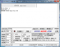
- COM port will receive the data read from and written to DataFlash.
SPI_Debug
SPI_NRF24L01
Demo Description
- This is a demo of NRF24L01 wireless communication.
Operation
Steps
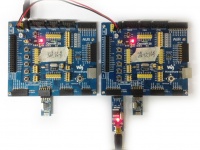
- Prepare two OpenM128 and two NRF24L01 boards, for sending, TX, and receiving, RX, data. The following is an example of 2 OpenM128 boards.
- Connect two NRF24L01 RF Boards[14] to the SPI interface of OpenM128 boards separately.
- Connect the RX board to a PC via PL2303 USB UART Board.
- Power up and download the program.
- Check your COM port and set baud rate to 9600.
Phenomenon
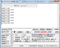
- COM port will receive the data from TX board to RX board.
T_C0_LED
Demo Description
- Control LEDs' status by I/Os and Timer 0(T/C0).
Operation
Steps
- Jumper LED_JMP ON.
- Power up and download the program.
Phenomenon
- 8 LEDs status will be toggled.
Photos
USART
Demo Description
- USART0:USART0 self-send-self-receive test.
- USART1:USART1 to send 'U' automatically.
Operation
Steps
- Connect PL2303 USB UART Board (mini) to UART0 (or UART1)
- Power up and download the program.
- Check your COM port and set baud rate to 9600.
Phenomenon
- USART0:The information sent by PC's COM port will be received from the same port.
- USART1:USART1 will send 'U' automatically.
USART_Printf
Demo Description
- COM port will receive the data from USART0 interface.
Operation
Steps
- Connect PL2303 USB UART Board (mini) to UART0.
- Power up and download the program.
- Check your COM port and set baud rate to 9600.
Phenomenon
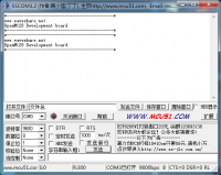
- The program will send data via USART0 automatically, and then, COM port will receive the data from USART0 interface.
References
- ↑ OpenM128 development board
- ↑ ATmega128A datasheet
- ↑ AVR programmer or debugger
- ↑ 4.0 4.1 2.2inch 320x240 Touch LCD (A): Please click in Graphic-Lcd for more details about touch LCD.
- ↑ 8 Push Buttons
- ↑ 8 SEG LED Board
- ↑ AD Keypad
- ↑ PL2303 USB UART Board (mini)
- ↑ AT24CXX EEPROM Board
- ↑ PCF8563 RTC Board
- ↑ FT245 USB FIFO Board (mini)
- ↑ LCD12864-ST (3.3V Blue Backlight)
- ↑ AT45DBXX DataFlash Board
- ↑ NRF24L01 RF Board (B)

